


How a CPU Microprocessor Is Made
This is a quick tutorial to help you understand how microprocessors and other integrated circuits are made, or 'fabbed.' Starting from a chunk of silicon and resulting in a device with millions and millions of transistors that now run almost everything in your life.
Making the Wafer
CPUs are made mostly of an element called silicon. Silicon is rather common in earths crust and is a semiconductor. This means that depending on what materials you add to it, it can conduct when a voltage is applied to it. It is the 'switch that makes a CPU work. Modern CPUs literally contain millions transistors.
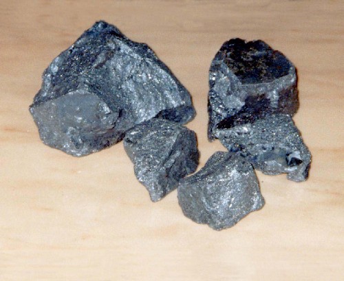
Raw silicon
The first stage in making a CPU is to make the wafers that they are built on. This process begins with the melting of polysilicon, together with minute amounts of electrically active elements such as arsenic, boron, phosphorous or antimony in a quartz crucible (a container that won't melt at high temperatures).
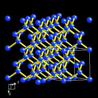
Silicon is a simple FCC Lattice (Face Centered Cubic)
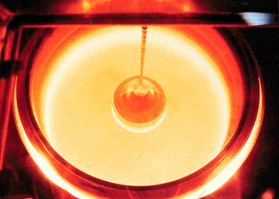
Once the melt has reached the desired temperature, we lower a silicon seed crystal, or "seed" into the melt. The melt is slowly cooled to the required temperature, and crystal growth begins around the seed. As the growth continues, the seed is slowly extracted or "pulled" from the melt. As the the ingot is pulled it is slowly rotated. This is done to help normalize any temperature variations in the melt. The temperature of the melt and the speed of extraction govern the diameter of the ingot, and the concentration of an electrically active element in the melt governs the electrical properties of the silicon wafers to be made from the ingot. This is a complex, proprietary process requiring many control features on the crystal-growing equipment. The crystals naturally tend to a circular shape due to the crystal structure itself, and the surface tension on the liquid.
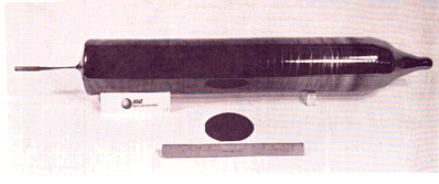
6" ingot is drawn out of the melt. This process can take several hours.
This results in a large ingot that looks like this:
To be useful the ingot must be very pure. The ends and edges are the areas of highest impurities (this is due to annealing) so the ends are cut off and the edges are ground down so the ingot is the proper diameter.
Wafers may then be heated to help remove any defects. (annealing)
The wafers are then inspected with a laser to find any surface defects.
The wafers are then inspected with a laser to find any surface defects.
A single crystal layer (epilayer) may then be added to the surface of the wafer.
The wafer is now ready for etching.
Etching
:confused:
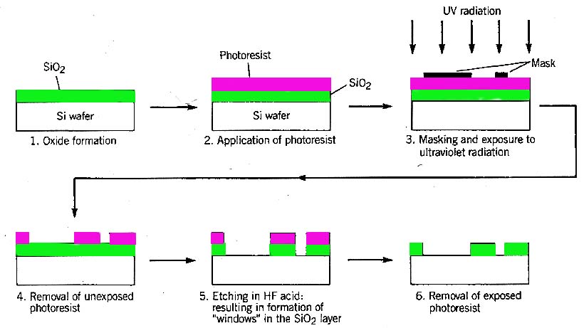
1. Oxide A layer of oxide is implanted on the wafer. This is most often done by exposing the wafer to steam at very high temperatures
2. Photoresist A layer of organic photoresist is applied. This is like film in a camera
3. Masking A mask is applied and UV light is shown through the gaps. UV light is now used because of its shorter wavelength. A shorter wavelength means that it can pass through a smaller mask. The UV light hardens (fixes) the photoresist.
4. Cleaning The unhardened mask is removed with an organic solvent
5. Etching Hydroflouric (HF) acid is used to etch away the Silicon Oxide. Since HF is inorganic it does not attack the photoresist.
6. Cleaning The remaining photoresist is washed away. The wafer is now ready for doping with another type of silicon. Or for adding contacts.
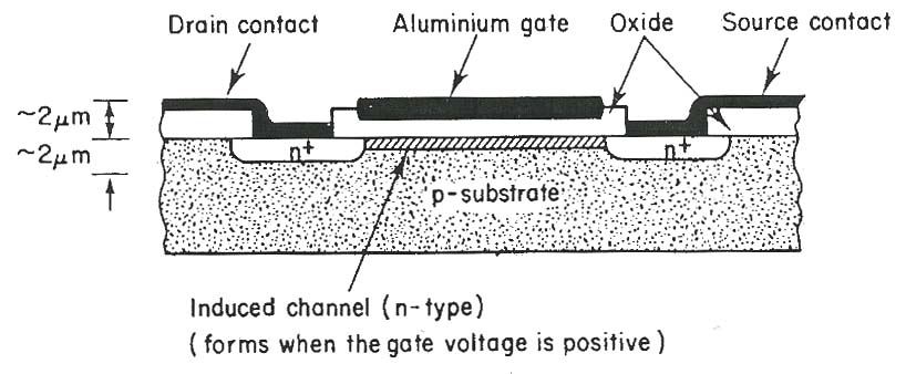
Making the tranisistor
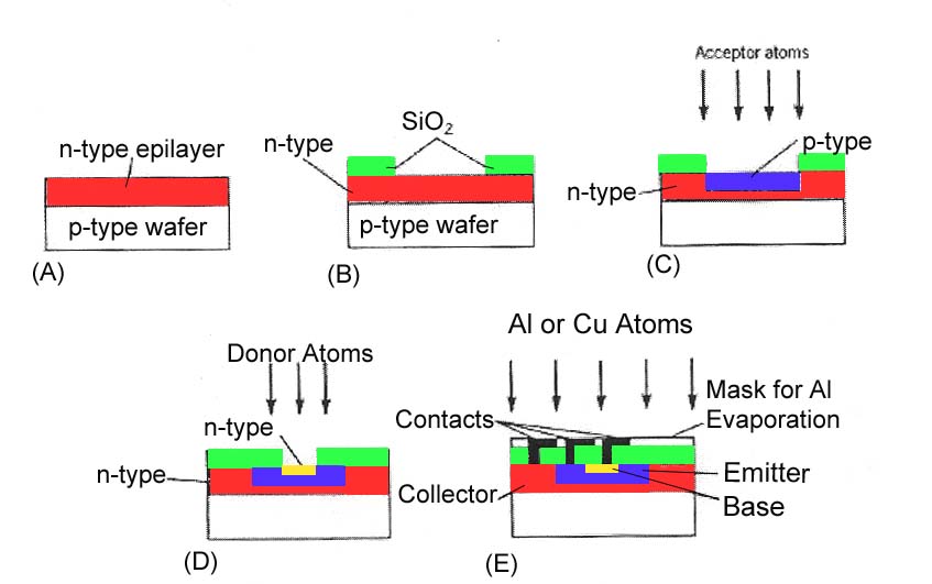
(A) A p-type wafer (silicon doped with Boron) has a epilayer of n-type (silicon doped with Phosphorous or Arsenic)
(B) A mask is used to implant Silicon Dioxide, for the insulator
(C) Acceptor atoms (Boron) are diffused into the window in the Silicon Dioxide
(D) Using another mask additional Silicon Dioxide is grown. and donor atoms (elements like Arsenic with excess electrons) are implanted.
(E) Another mask is used to grow additional Silicon Dioxide. ANother mask is then used to implant evaporated Aluminum or Copper for the contacts. This is a Bipolar Junction Transistor (BJT).
These transistors are what are used in microprocessors and memory. They take less power then BJTs but are made in the exact same way.
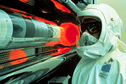
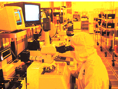
This work is all done in 'clean rooms' as even the smallest particle of dust can wreck a whole chip!!
The workers wear 'bunny suits' to keep dust and skin particales from getting into the air.
These days much of the process is automated so the technicians have to monitor alot of sophisticated machines.
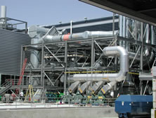
A fab requires large amounts of infrastructure to deal with all the chemicals, high temperatures, and pressures.
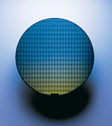
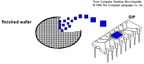
Once the wafer full of chips is made each chip is tested while stll on the wafer. If a bad one is found it is marked so that it is not used. Most bad chips tend to be areound the edge of the wafer. The best chips are in the center and are sometimes selected for extended temperature testing for military or industrial use.
The wafer is then cut up into its individual chips. These chips are what gets 'bonded' to the packge that is in your computer.
Typically the bonding is done in countries where labout costs are low. The facilities to do so can be quite large.
This is an assembly facility in Costa Rica.
Thie final product may take 3 months to complete
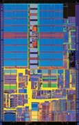
A CPU with 25+ million transistors is impressive by any standards.


المفضلات